Files
| Files | |
|---|---|
| CAD | |
| Images | |
| switch_mon | |
| .gitignore | |
| LICENSE | |
| README.md |
README.mdView this project on CADLAB.io.
gbaZero
One day I decided to buy a broken Gameboy Advance, gut it, and replace the innards with a Raspberry Pi powered board. This style of project has been attempted before in custom plastic (see Game Grrl and its derivitaves) and Nintendo plastic (see Ryzee119's project and Game Pie Advance). Here's a little build log for my version of this project.
Design
The design process was mostly me sitting at my desk doing research and CAD work in Inkscape and EAGLE.
To get the right PCB shape, I desoldered all the parts from a sacrificial PCB and took a 600dpi scan of it.
That scan was then traced in Inkscape, and the resulting SVG was imported into EAGLE using cmonr's svg2poly ULP.
I wanted the wacky button footprints to be just like Nintendo's. I had a scan of the footprints open in an image viewer, overlaid an EAGLE window made transparent by Peek Through, and traced out the shape using the polygon tool. It's kind of like a high tech lightbox.
Ultimately I threw my work on the board shape and drilled holes out the window in favor of the shape from Ryzee119's project. I was almost guaranteed to mess something, and their's was already tested to be the right fit, so that seemed safer. I was also unaware of Ryzee119's project when I started all the scanning and tracing. I did keep the Nintendo-esque button footprints.
Assembling the Hardware
Power Circuitry
It turns out using someone else's work is often easier than doing it yourself. In this case, I used a PowerBoost 1000C to manage charging the battery and supplying power for this board. It's a capable little board, so all I had to do was desolder the JST battery connector to trim the height and cover the backside with electrical tape because it will sit flush on the main board.
Here's the power circuit all soldered up. I'm using a common anode tricolor LED and some NOR gates and inverters to display the GBA's state (powered on, charging, or low battery). The logic ICs are in the top left and the LED is on the other side of the board.
The switch in the bottom right was salvaged from a broken GBA. I couldn't find where to source a replacement for the life of me. The resistor and diode in the bottom right are a way to have the Raspberry Pi power off cleanly. Sure, one could just cut power to the Pi, but that puts the SD card at risk for corruption. The Enable pin on the PowerBoost is tied to both the switch and a GPIO (through a diode, so the GPIO doesn't get backpowered), so when the Pi boots it holds the PowerBoost on, even if the switch is turned off. Flicking the switch off does trigger a shutdown script, which shuts down cleanly and disables the PowerBoost at the end.
Uhoh, notice those ugly wires coming off the logic ICs in the previous image? Turns out I either used the wrong footprint in EAGLE or ordered the wrong package part from Digi-Key. Either way, it needed some bridging. I realized I could take pictures with my phone through the stereo microscope in the lab, so I did. I trimmed the wires after this shot, and cleaned up the extra flux too.
There's nothing like a little hot glue to keep everything in place!
Ta-da! The LED works and is in the right place for the light pipe. It may be a little too bright, but that's nothing a larger current limiting resistor can't fix. The LED is blue when the unit is powered on, green when it is charging, and red when the battery is low. The one wrinkle is that the LED is off when the unit is off, but charging. The original design assumed a common cathode LED instead of a common anode LED, which is what I ended up finding on Digi-Key. Rather than redo the logic, I just threw an inverter on at the end. Unfortunately the inverter was powered by the regulated voltage, so it doesn't invert unless the unit is on. Had the LED been common cathode, it would have been driven by the 5V USB charging voltage. Ah well.
Also of note, the board uses the original Link Cable connector and a custom cable for charging. The Raspberry Pi's RX and TX pins are also exposed on the Link Cable connector, so with an FTDI cable one can log into a terminal and fiddle around with the system. This ended up being way more convenient than SSHing into the system over wifi.
Display Circuitry
Remember that part about using someone else's work? I'll call it standing on the shoulders of giants. Turns out Adafruit sells a 2.8" Raspberry Pi display which fits pretty perfectly in a GBA. I took the circuitry from their board and transposed it onto mine. Should work perfectly, right? Yeah, we'll get to that.
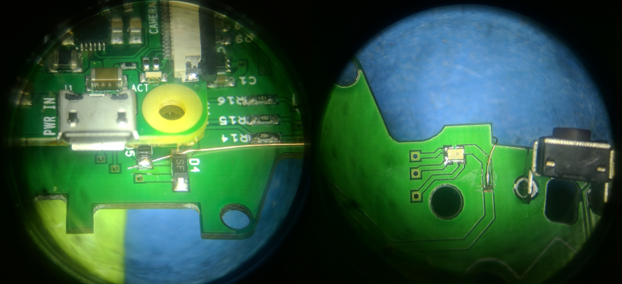
Here's a gratuitious microscope shot. The display connector had 0.5mm pitch pins, which is the smallest thing I've soldered. Solder braid makes everything look super clean (and not bridged).
Oh yeah, I was going wild with that microscope. There's actually a problem in this picture. I'll get to that shortly.
Transposing a circuit only works if you do it correctly, which I did not. I crossed the I2C lines which send touchscreen data to the Raspberry Pi, so I had to cut those traces with a knife and reroute them with magnet wire. Those are the two wires going off the edge of the board. That didn't matter so much as I wasn't using the touchscreen anyway, but I like to be proper. The bigger issue is that I completely missed a trace that had been connected with a 0 ohm resistor on Adafruit's board. That was fixed with the third magnet wire running from the display connector to U1. I opted for kapton tape instead of hot glue to hold these fixes in place.
There was another issue with the display circuitry that prevented an image from being displayed, hinted at before. U1 is an APX803 voltage supervisor on a 3.3V line. However, I bought an APX803 which had a 4.63V threshold. D'oh. The Adafruit schematic didn't note the treshold level, and I must not have been paying much attention while filling my shopping cart. In lieu of ordering another supervisor, I stole the one from the Adafruit board and dropped it on mine.
Ta-da! With a few magnet wire fixes and a new supervisor, there's an image! This testing and debugging was done after all the parts were soldered, so these images aren't quite in chronological order. It would be hard to display anything without the Raspberry Pi.
Audio Circuitry
While most Raspberry Pis have audio output, the Zero does not. It's the cost to pay for a tiny $5 board. Luckily, it can still output a PWM audio signal. A little RC filtering and amplifying later, and it should be good to go. The headphone jack and volume potentiometer were new parts. A minor annoyance, GND and 5V are swapped on the volume potentiometer, so rotating it towards max volume (according to the plastic shell) makes it quieter.
Here's a microscope shot of the buffer and five passives that make up the filter. The design was taken from the Raspberry Pi 3 schematic. Once again, there's a problem in here. More on that shortly.
The amplifier is an LM4875. That amp only does mono sound, but it can automatically switch between a speaker and a headphone jack. An earlier design had a separate analog switch IC which could handle stereo output, but was way more cumbersome. The GBA only has one speaker anyway (though headphones have two).
So about that problem, when I went to test the audio, the speaker got hot. As a colleague said "you can't hear DC," and indeed there was an unexpected DC voltage across the speaker. The Raspberry Pi 3 schematic I copied the audio circuitry from had a pulldown resistor right before the audio jack. This is great for headphones or speakers or what-have-you, but terrible for amplifier input. In fact, the LM4875 datasheet says to put a 0.22uF capacitor in line with the input signal to get rid of incoming DC voltage, which I did not do. All that had to change was to remove the last pulldown resistor before the amplifier and let the last capacitor filter out all the DC voltage. You can see R12 hanging off into nowhere, just so I wouldn't lose it.
This took me forever to figure out, and in fact the solution was proposed by a colleague who earned his name in the silkscreen for version two. Some failed debugging attempts were powering the audio circuitry with 3.3V instead of 5V (the cut and solder blob in the top left), replacing R13 with a wire, dis/reconnecting the volume potentiometer, and changing bypass capacitor values (C7 is two stacked capacitors in the picture above). Gross.
Raspberry Pi Zero
Soldering on the Raspberry Pi proved to be the one part of this project that went as expected. First I soldered on a 40 pin SMD connector.
Then I taped the bottom of the Raspberry Pi, since it would cantilever over the PowerBoost.
Then I soldered it on the header. All good! This picture was taken after the display debugging, so you can see where those two magnet wires ended up. I also made a note to myself on the circuit board, seemed easier that way.
By now, the shoulder buttons had also been soldered on. I tried to use the original buttons to have a realistic feel. The buttons were tactile switch, but the plunger was made of a flexible rubber rather than a hard plastic. Unfortunately, one of the switches would not switch at all. I don't know what this poor Gameboy went through in a prior life, but it could not have been good. We had one 90 deggree tactile switch in the office, so I bent it's pins and jammed it on the board, which worked just fine. The shoulders currently have an asymetrical feel though, which kind of drives me nuts.
It Lives!
At the end, everything get put in the salvaged plastic, and yes, it runs Doom! I popped off the old display lens because it was so roughed up and the Adafruit display can hold it's own.
The Plastic
There are tons of Gameboy Advance shell replacement kits available on Amazon, so it seemed right to replace the scarred purple shell. I went with yellow because my first Gameboy, a Color, was yellow. Thanks Mom & Dad!
The plastic has all sorts of interior supports for the cartridge and battery, but those need to be removed here.
A dremel probably would have worked wonders here, but I opted to "cut" the plastic away with a soldering iron. Melted ABS fumes aren't pleasant (or healthy), so this work was done under a vacuum.
The battery compartment was a little trickier to remove partially because it was larger and partially because I had to remove material close to that bottom edge. I ended up applying a little too much heat and the bottom edge warped a bit. It's not bad enough to prevent the shell from fitting, but you can see it from the outside if you're looking for it. Plus I know it's there. Dang.
The display is held in place with the thinnest double sided foam tape I could find on Digi-Key. I finally removed the film protecting the screen before mounting, and boy does it look clearer. It's not easy to finagle the ribbon cable into the connector when the display is mounted, but it's doable.
And voila! The display lens has been installed and I'm done. What better way to celebrate than with the greatest first person shooter of all time, Chex Quest?
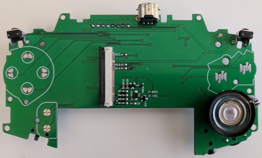
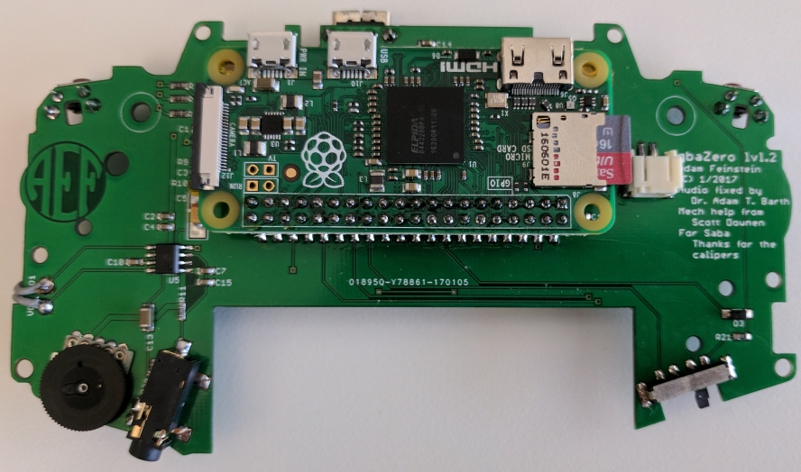
PCB v2
I wasn't really happy with the IC pad size for the power LED logic, or the asymmetrical shoulder buttons, or the fix wires for the display, and I wanted to try out Seeed Studio's PCB Assembly service, so I recruited a few friends to defray the cost for a batch of 10 PCBs fixed the layout, and had them built. Seeed Studio couldn't assemble the whole board, but it was quite nice not having to solder everything. Here it is in all its glory.
But of course there was something still broken (hardware is hard). Even though the power LED's logic gates are still powered when the unit is off but charging, the LED itself is not. Nothing a wire couldn't fix. This one I'll have to live with.
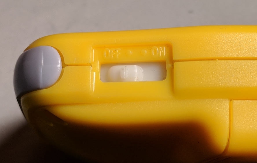
I noticed some odd behaviour when trying to turn on and off the gbaZero v2 PCB as well. After a little investigation, it turns out that the original GBA power "switch" was actually a linear potentiometer. Seriously Nintendo? It kind of works as a switch, but not always, which is why I hadn't noticed until now. I'm not planning on a v3, so I scoured Digi-Key for a switch with the same footprint and managed to find one. The actuator dimensions were slightly off, so I had to 3D print a new piece. Works like a charm!
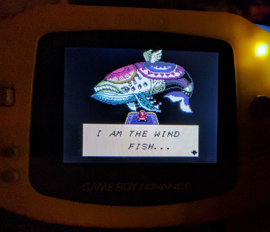
At the very end of the project, the Wind Fish is saved! I found that deeply satisfying.
The Software
Software doesn't get pretty pictures, sorry.
I connected a USB wifi dongle to the Raspberry Pi using a USB OTG cable and configured with these instructions. I only used wifi during configuration.
The base OS is Adafruit's version of Jessie Lite, with kernel drivers for the display already built in. RetroPie was installed on top of that, which handles all of the game playing. I also used another of Adafruit's guides to install fbcp, necessary to draw to the display from RetroPie.
Retrogame was used to map the button GPIOs to actual key input. I had to further modify the mappings in Emulationstation (a part of RetroPie) because some games expected key combinations that happened to do other things, like quit the game.
Wiring Pi was used to set and monitor the power switch GPIOs.
These instructions enabled auto-login, and these instructions started Emulationstation automatically.
One hiccup was that initially there was no audio output, even though it was set to play over the "3.5mm jack" instead of HDMI. The solution? Unmute the audio. Occam's Razor hard at work.
The other hiccup was a hardware failure. Every once in a while, though with increasing frequency, the Raspberry Pi wouldn't boot, but would print "mmc0: fsm 1, hsts 1" to the terminal in an infinite loop. Turns out the SD card was busted and had to be replaced. Good thing I made a system image after tweaking the install to my liking.
Final Thoughts
Hardware design is hard, and not everything can be fixed in software. Most of the janky fixes from the v1 PCB were fixed in the v2 one, but it's still not perfect. If only fabricating a board was as easy as typing "make." Also, Link's Awakening DX is still awesome.