Files
-
hardware / powerSupply_kiCad / power_supply.kicad_pcb
-
hardware / powerSupply_kiCad / power_supply.kicad_sch
-
hardware / powerSupply_kiCad / power_supply_simulation.kicad_sch
-
hardware / sensor_KiCad / accel.kicad_pcb
-
hardware / sensor_KiCad / accel.kicad_sch
-
hardware / workerBoard_kiCad / ad7768.kicad_sch
-
hardware / workerBoard_kiCad / ADC_RS_MCU.kicad_pcb
-
hardware / workerBoard_kiCad / ADC_RS_MCU.kicad_sch
-
hardware / workerBoard_kiCad / driver0-3.kicad_sch
-
hardware / workerBoard_kiCad / thvd8000.kicad_sch
-
hardware / workerBoard_kiCad / Vref.kicad_sch
| Filesdochardware | |
|---|---|
| .. | |
| Assembly.md | |
| Assembly.pdf | |
| PCB.md | |
| PCB.pdf |
PCB.mdPrinted circuit board details
Main board (ADC_RS)
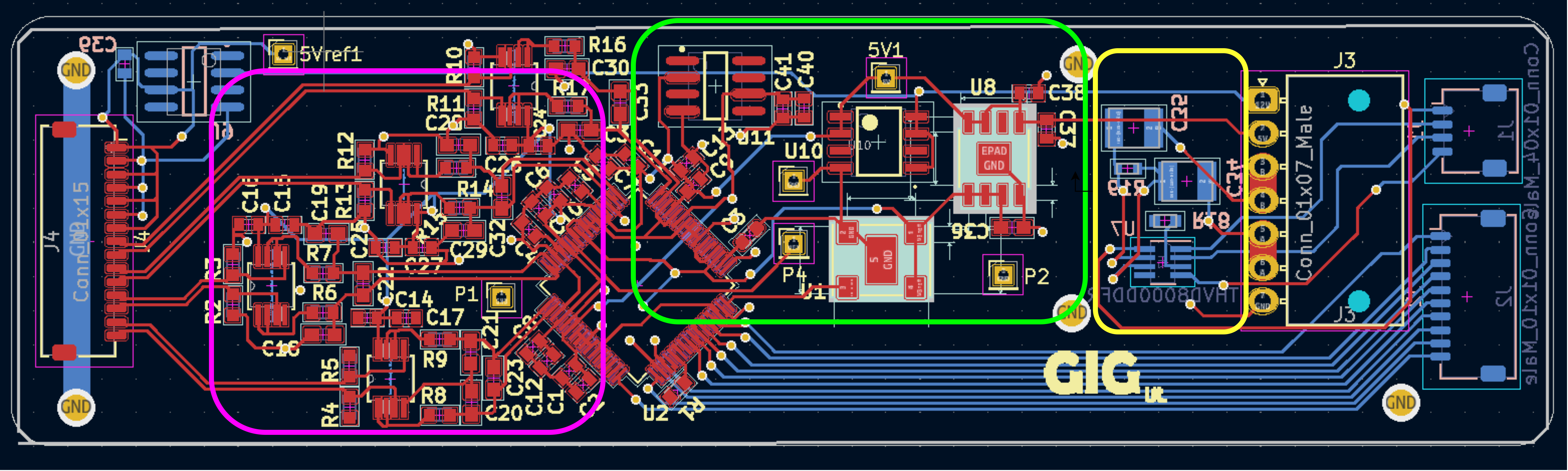
The components have been divided on 3 different printed circuit boards (PCB). The main board contains the ADC, the MCU and the communication module. This board has 4 layers in order to reduce its size as much as possible and to ensure a decoupling between the digital signals, the analog signals and the power supply. Its dimensions of 40 by 160 mm respects the objective of a diameter less than 46 mm. The Altium version contains micro-vias, which is more costly to produce. This version is deprecated and is present here only for reference. The active board is the KiCad version, which doesn't have micro-vias.
ADC drivers (pink)
Those are 2 channels amplifiers with unity gain to drive the ADC analog inputs. They are ADA4841-2 from Analog Device. The output of a sensor has 2 signals. Both signal are conditioned by an amplifier before going to the ADC. The design of this amplification stage is based on the application note https://www.analog.com/media/en/technical-documentation/application-note....
Voltage regulator (green)
4 different voltage regulator are used on this board. The 4.096 V is used as a reference for the ADC. The 3.3 power up the clock and reference the ADC. The 5Vref is the reference for the sensors and it is a high precision voltage regulator while the 5V is used to power up the ADC and other component, he can produce higher current than the 5Vref.
RS-485 (Yellow)
The THVD8000 is responsible of transforming the UART data to a frequency modulated RS-485 signal that is send on the A and B line. The carrier frequency is set by the R22 resistors. Values of resistor can be found in the THVD8000 datasheet. The choice of the decoupling capacitor is based on the application note here THVD8000 design guide.
Connectors
J1 is dedicated to the communication chip. Theses wire have to be connected to the chosen MCU. J2 is a 10 pin connector dedicated to the configuration and communication with the ADC. J3 is a 7 pin high power connector used by the A,B and 12V lines. Finally, the J4 15 pin connector is used to drive and collect the signals from 4 analog differential sensors.
Power supply
The power supply and its component are built into a separate 40 by 85 mm PCB. This way, switching noise cannot affect the precision components of the main board. The design is based on the DC2895A demo board. On one side the A and B line enters and goes thru the inductor to filter out the high frequency. Since the cable is expected to have a high capacitance (140 microF), turning on the power supply can create a current surge. The added 100 Ohms resistor (R5) allows to reduce the current spike when turning on the power supply. The mode header is used to set the operating mode for the output of the power supply. Burst mode is the default since it draws less current.
Sensors
The sensors are assembled on miniature PCBs in order to facilitate the assembly on a mount with the desired geometry. Wires are soldered directly into the sensor boards. These wires are linked to the main board by a locking clip connector to ensure proper contact The PCB follows the connection proposed in the sensor datasheet (si1521L).